
Electronics and Semiconductors
Instruments provided by Bettersize offer particle size and shape analyses of the raw materials of electronic products.
In the electronics industry, many materials and processes have strict requirements for particle size and particle shape. For example, the silicon carbide powder used for cutting silicon wafers requires a tight particle size distribution and a sharp particle shape corner angle, the cerium oxide abrasive used for polishing requires a small particle size without large particles, and the silica dioxide materials used for sealing integrated circuits require strict standards for the particle size distribution and spherical degree. Particle size and particle shape analysis is a basic method of production and product quality guarantee in the electronics industry.
During the research, design, manufacturing and quality control of electronic components, the instruments provided by Bettersize can help you to realize material properties, including:
● Guaranteeing CMP slurry quality.
● Guaranteeing particle size and particle shape of milling for cutting and polishing.
● Guaranteeing the quality of integrated circuit sealing materials.
Citations
- Bettersizer 2600
Functional redundancy as an indicator for evaluating functional diversity of macrobenthos under the mussel raft farm near Gouqi Island
DOI: 10.1016/j.aquaculture.2023.740024 Read Article Zhejiang Ocean University | 2024Biological traits analysis (BTA) helps to evaluate the effects of different environmental variables on the traits-based functional composition of macrobenthos. However, research on functional traits of macrobenthos under mussel farming is limited. We investigated the spatial and temporal response of the benthic system in terms of taxonomic and functional diversity to environmental variables of farming and natural stressors resulting from suspended mussel farming near Gouqi Island of eastern China Sea. The functional traits of macrobenthic assemblages under mussel farming were characterized by “medium adult body size”, “vermiform body form”, “high flexibility”, “infauna”, “semi-motile”, “gonochoristic”, “surface deposit-feeders”, “carnivores”, “semi-motile burrowers”, and “tube-dwellers”. Functional redundancy was stable in response to mussel farming stresses among seasons, whereas species diversity showed efficient to evaluate natural variables. Functional diversity was significantly affected by farming stressors rather than natural variables, Further analysis using multivariate methods together with continuous monitoring were highlighted to evaluate the impacts of mussel farming. Our results reinforce the importance of macrobenthic species and functional traits analysis to evaluate human stresses driven impacts in offshore ecosystems. By analysing the environmental variables with different sources, independently, we concluded the main effects of human pressures on macrobenthic community. Such distinction could be particularly effective to isolate variable environmental descriptors and evaluate their effects on functional diversity, making the current approach promising for the evaluation of ecological effects of anthropogenic stressors in aquaculture areas.
 - Bettersizer 2600
Degradation characteristics and utilization strategies of a covalent bonded resin-based solid amine during capturing CO2 from flue gas
DOI: 10.1016/j.seppur.2023.125621 Read ArticleChina University of Petroleum | 2024In this study, various types of degradation as well as attrition which are possibly encountered in a circulating fluidized bed temperature swing adsorption (CFB-TSA) process, were conducted experimentally to evaluate the stability of a resin-based solid amine sorbent. Other characterizations methods, such as elemental analysis (EA), Fourier transform infrared spectroscopy (FTIR) etc. were applied to further reveal the degradation mechanisms. The results showed that thermal degradation occurs from 140–160 °C due to the decomposition of amine group. The CO2-induced degradation occurs from a higher temperature of 160–180 °C accompanied by the production of urea. Hydrothermal stability is good below 130 °C, but the ionic impurities in steam crystalized on particle surface can accelerate the degradation. Oxidative degradation is the most harmful, which starts at a lower temperature of 70–80 °C with the formation of aldehyde. The existence of H2O in atmosphere can alleviate the oxidative and CO2-induced degradations. The employed sorbent has a very low attrition index of 0.05, which is 1–2 orders lower than typical commercial fluidized bed catalysts. Based on the results of stability evaluation, some design suggestions for proper utilization of this sorbent or other similar resin-based sorbents have been provided in an industrial CFB-TSA process.
- Bettersizer 2600
De-branching of starch molecules enhanced the complexation with chitosan and its potential utilization for delivering hydrophobic compounds
DOI: 10.1016/j.foodhyd.2023.109498 Read ArticleShihezi University | 2024The current study aimed to prepare the complexes between debranched-waxy corn starch and chitosan polymers (DBS-CS), and then investigated their corresponding structural characteristics, rheological property and potent application in Pickering emulsion. The results indicated that the existence of chitosan significantly inhibited starch short-range molecular rearrangement for all DBS-CS samples, which was manipulated by both debranching treatment and chitosan content. Interestingly, this is the first study to reveal that the outstanding peak at 1.8 ppm in 1H NMR spectrum for sample DBS-CS was gradually shifted towards a lower-field region following an increased chitosan content. Moreover, the debranching treatment shifted the crystallinity pattern from A-type to B-type and the relative crystallinity of DBS-CS decreased gradually with the increased content of CS. All samples had a pseudoplastic fluid and shear-thinning behavior with an enhanced shear resistance following the complexation. The DBS-CS was applied in a Pickering emulsion for showing a greater emulsifying stability and a lower gel strength than native NS-CS prepared emulsion. Importantly, the encapsulation ability of curcumin in the DBS-CS emulsion was significantly improved, followed by an increase of 15.45% for its corresponding bioavailability compared to the control. Therefore, this study might highlight a potential carrier for delivering the bioactive substances in a green pattern. - Bettersizer 2600
Heat-induced aggregation behavior of wheat gluten after adding citrus pectin with different esterification degree
DOI: 10.1016/j.foodhyd.2023.109420 Read ArticleGansu Agricultural University | 2024Wheat gluten aggregation during heat treatment is beneficial to the final quality of gluten-based products. Exogenous pectin can affect gluten aggregation. However, the effect of pectin with different degrees of esterification on the heat-induced aggregation behavior of gluten and its possible mechanism are still unclear. Thus, the heat-induced aggregation behavior of gluten after adding pectin with different esterification degree was studied in this study. When the temperature was raised from 25 °C to 95 °C, pectin affected gluten aggregation and was related to the degree of esterification. Specifically, the results of rheological properties and particle size indicated that low-ester pectin improved the viscoelasticity of gluten and promoted gluten aggregation. Thermal properties revealed that enthalpy of gluten added with low-ester pectin (37%) increased from 92.96 J/g to 95.40 J/g during heating process. Structurally, the fluorescence intensity and surface hydrophobicity of gluten added with low-ester pectin (37%) were lower than those added with high-ester pectin (73%). In addition, low-ester pectin (37%) significantly increased the disulfide bond content (from 15.31 μmol/g to 18.06 μmol/g) and maintained β-sheet content of gluten compared with gluten alone at 95 °C, indicating that low-ester pectin was more likely to induce gluten aggregation. However, scanning electron microscope showed that the gluten added with low-ester pectin (46%) exhibited a denser network structure at 95 °C than that added with low-ester pectin (37%). These results will provide a theoretical base for the regulation of gluten aggregation and the quality of gluten-based products by pectin with different esterification degree.
- 1
- 2
- 3
- 4
- 5
- 6
- 84
Curated Resources
- Application Note
 bigClick
2025-01-09
Surface Cleanliness Detection of Silicon Substrates by the BeVision M1 Static Image Analyzer
Related Particle Size Analyzer

Bettersizer 2600
Particle Size Analyzer
Measurement range: 0.02 - 2,600μm (Wet dispersion)
Measurement range: 0.1 - 2,600μm (Dry dispersion)

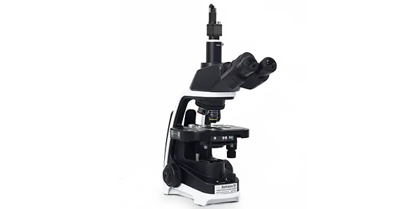
BeVision M1
Automated Static Image Analyzer
Dispersion type: Dry
Measurement range: 0.3 - 10,000 μm
Technology: Static Image Analysis
BeVision S1
Classical and Versatile Static Image Analyzer
Dispersion type: Dry & Wet
Measurement range: 0.3 - 4,500 µm
Technology: Static Image Analysis
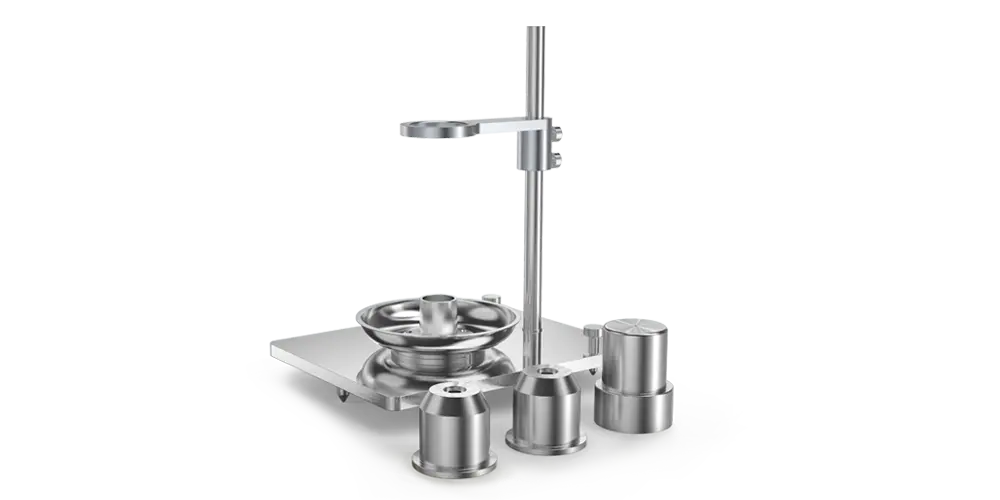
BeDensi B1
Bulk Density Tester
Measurement: Bulk Density(coarse powders)
Compliance with GB/T 16913
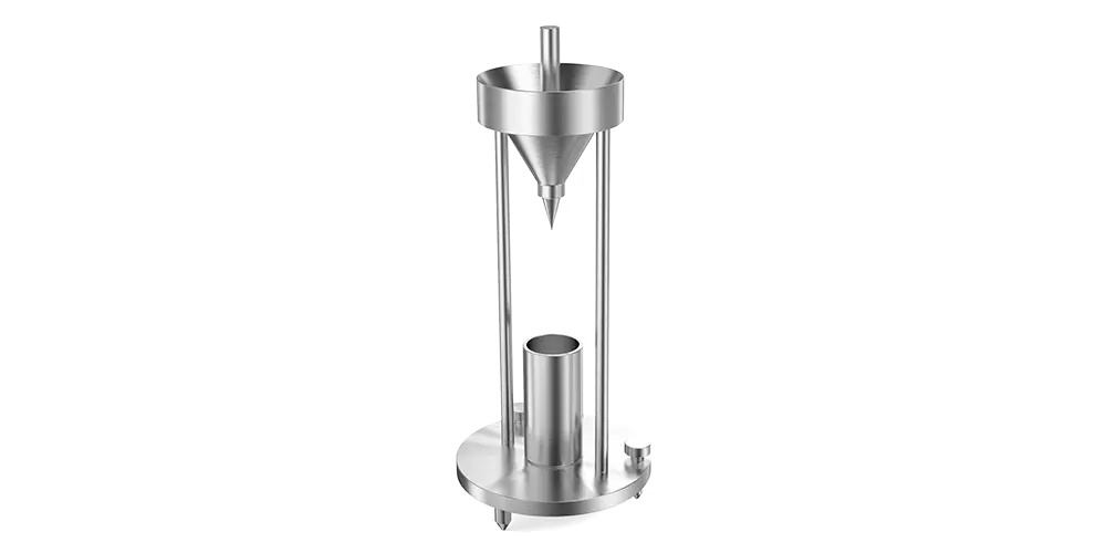
HFlow 1
Flowmeter Funnel
Measurement: Bulk density and Flow rate
Compliance with USP, Ph. Eur., ASTM, and ISO standards

BeNano 180 Zeta Max
Nanoparticle Size and Zeta Potential Analyzer
Particle size measurement via sedimentation technology
Refractive index measurement
Particle concentration measurement